石墨材料在半导体制造中还可以用来制造晶体管的封装。晶体管封装是将晶体管芯片密封在具有高度传导性的材料中,以保护晶体管不受外部环境的影响。在制造封装材料时,需要使用到石墨材料,其具有优异的机械强度和导热性能,能够有效地保护晶体管芯片。
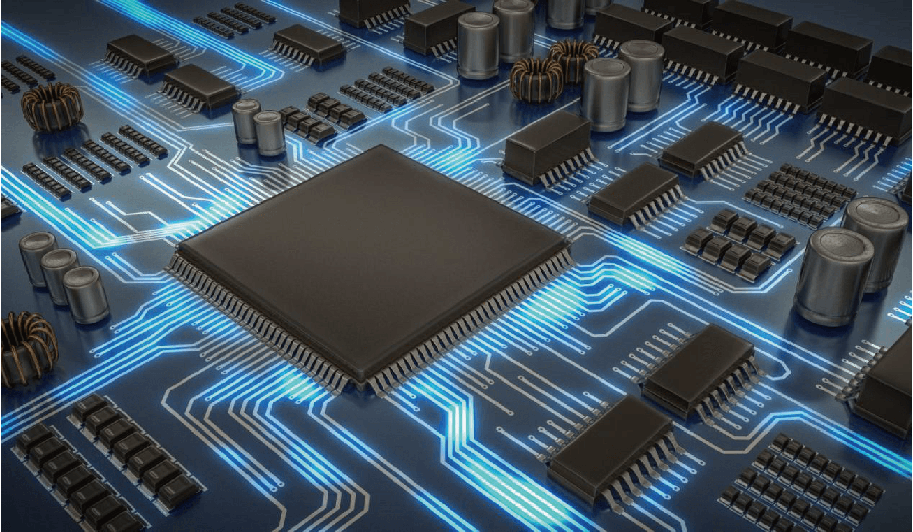
Graphite materials can also be used in semiconductor manufacturing to make transistorpackaging. Transistor packaging is the sealing of transistor chips inhighly conductivematerials to protect transistors from the external environment. In the manufacture ofpackaging materials,graphite materials are required,which have excellent mechanical strength and thermal conductivity, and can effectively protect transistor chips.